Trusted Partners & Collaborators


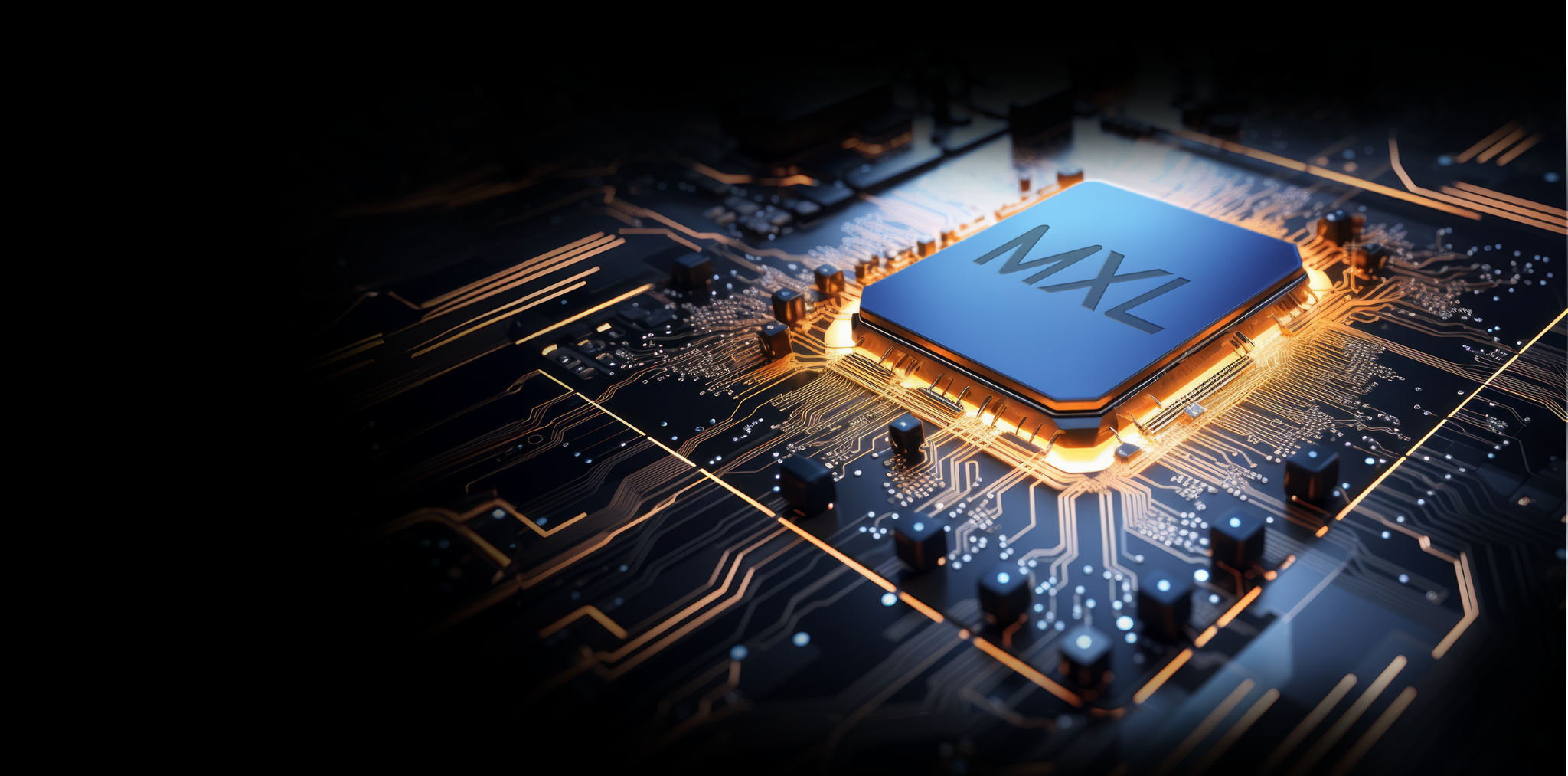
THE THERMAL CRISIS
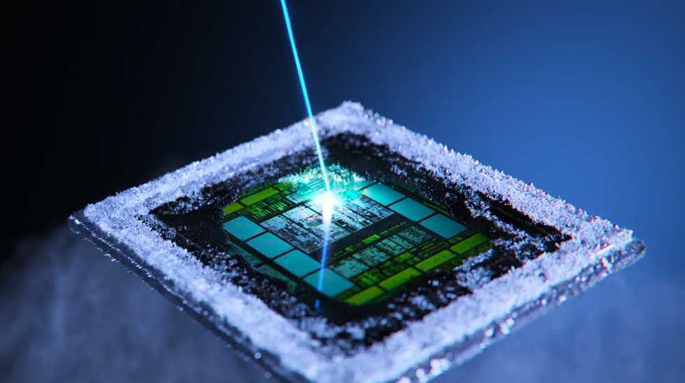
WHY AI HAS A CEILING
AI Is Running
Into a Wall
It Built
Itself.
AI is the most power-hungry technology ever built — and it's getting worse every year. More power means more heat. More heat means chips throttle themselves to survive. And the only fix is a more powerful chip that generates even more heat. This isn't a temporary engineering problem. It's a closed loop with no exit.
FORCE 01
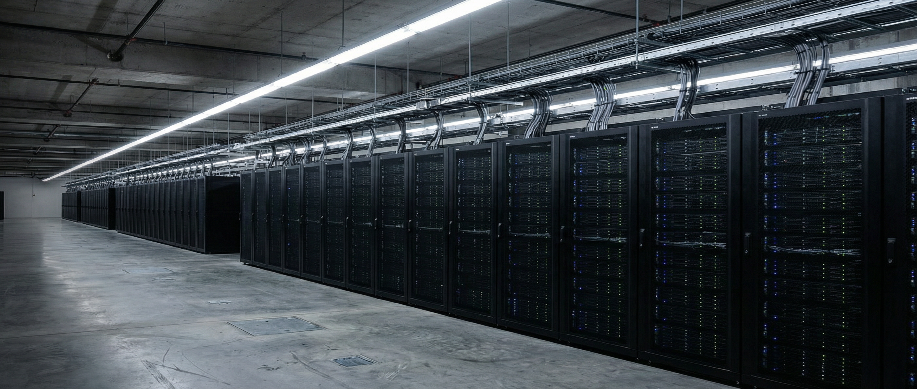
Energy
AI chip power draw has grown 7× in a decade — from 300W to over 2,000W per GPU. Data centers now consume more electricity than many nations, and demand is accelerating with no plateau in sight.
DRIVES
FORCE 02
Heat
Transistor-level hotspots now exceed 20 W/mm² — already pushing the limits of liquid cooling. By 2030, that number reaches 50+ W/mm². No fluid-based system can follow that trajectory.
LIMITS
FORCE 03
Performance
Heat forces up to 50% of chip area to remain powered off — dark silicon. Clock speeds are throttled. The performance AI demands is being actively strangled by a thermal ceiling that keeps getting lower.
THE LOOP CLOSES HERE
No Way Out. Until Now.
More performance demands more energy. More energy generates more heat. More heat destroys performance. There is no exit — unless you break the physics.
THE NUMBERS — HOW FAST IT'S COMING
Industry Impact
ONE TECHNOLOGY.
MANY FRONTIERS.
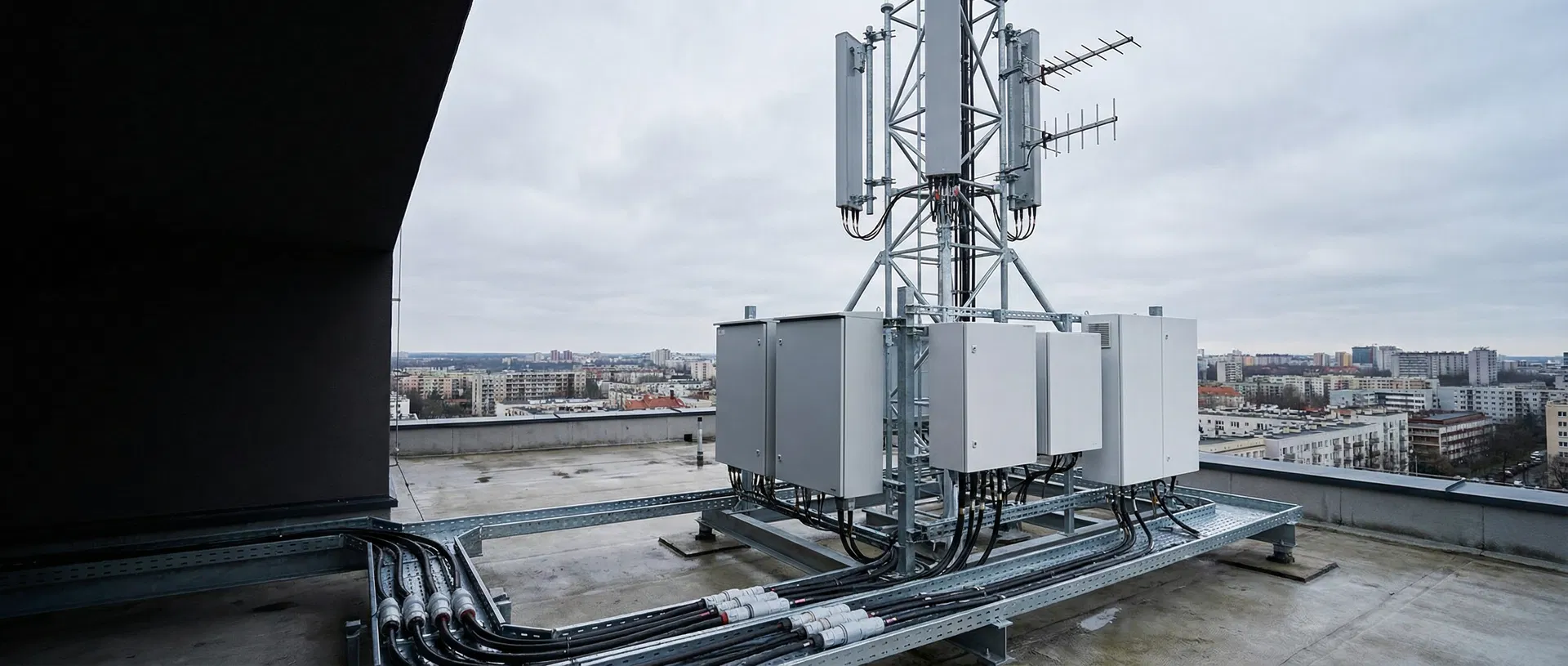
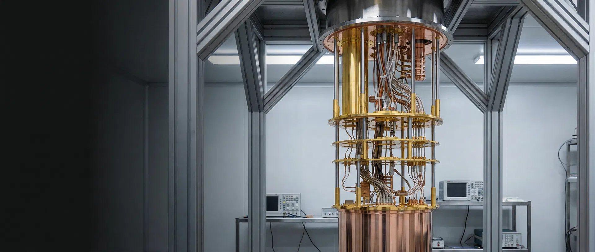
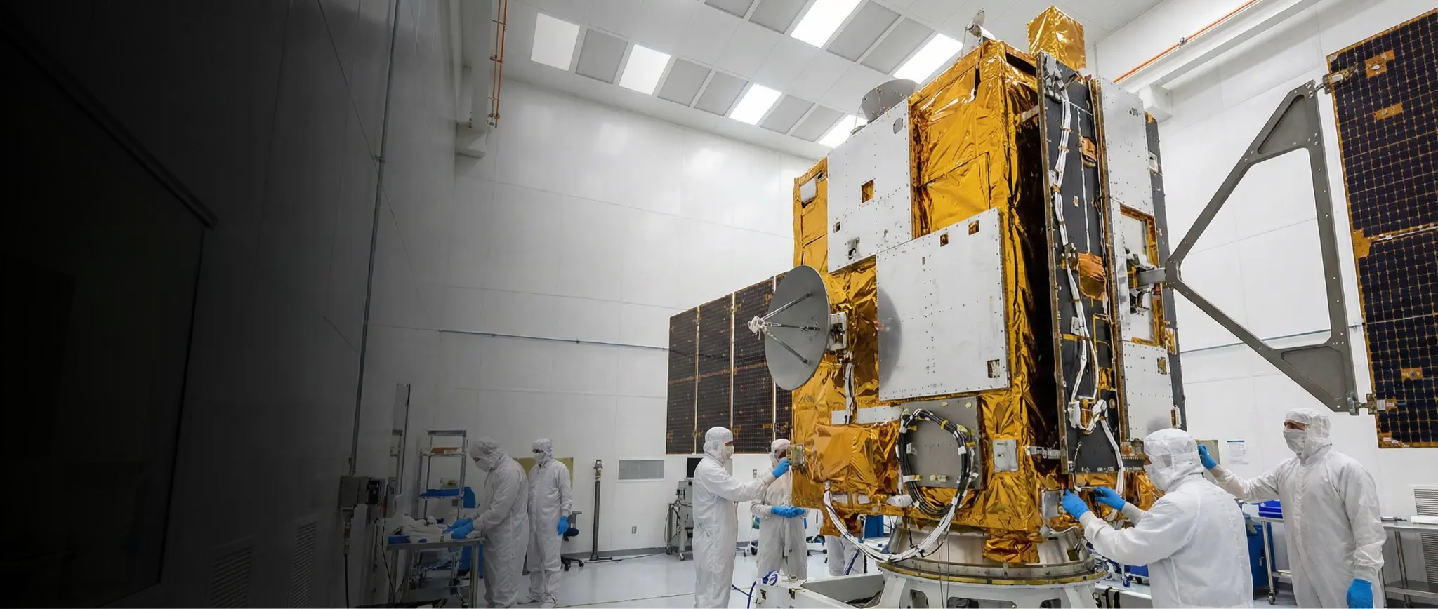
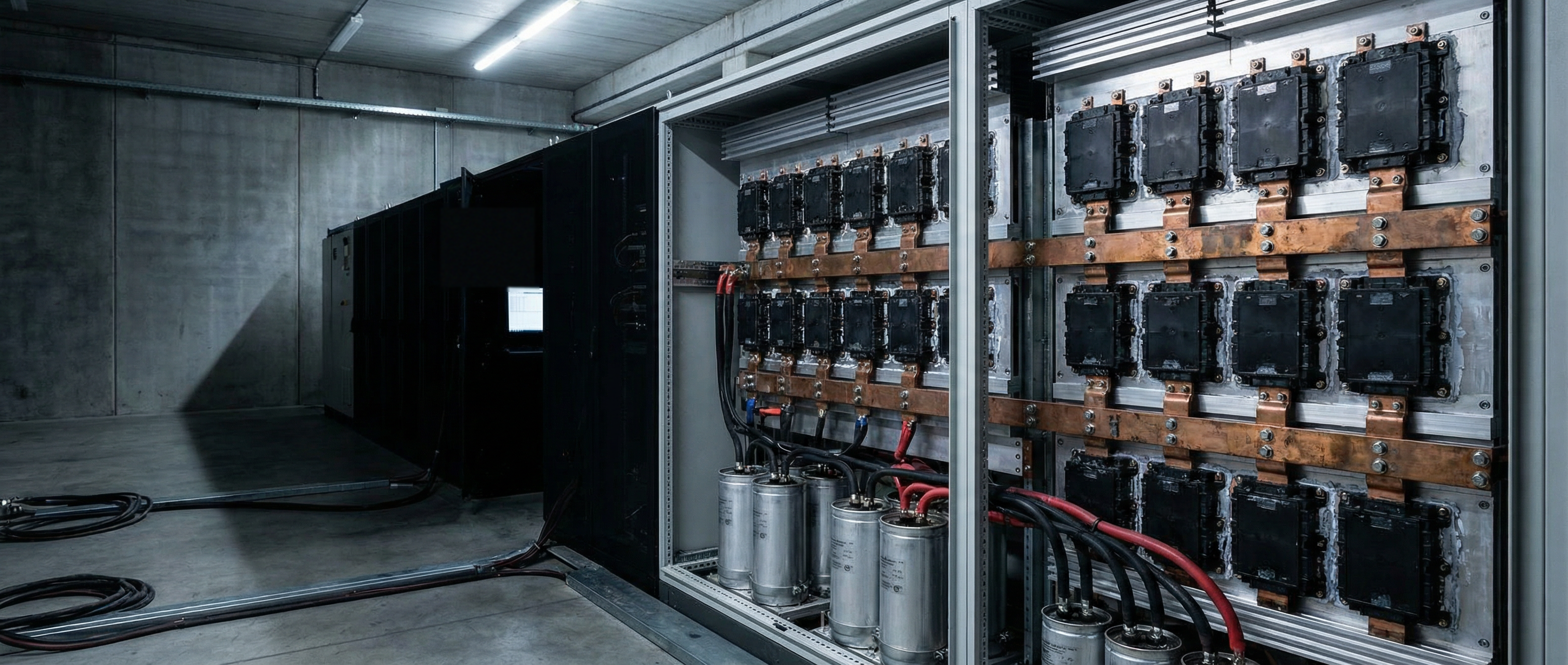
Six sectors where thermal limits are the binding constraint on performance, reliability, and scale — and where Photonic Cooling changes what is possible.
Leadership
The Founding Team.
Physics, HPC, and Growth.

Jacob Balma
Founder & CEO
Former HPC architect at Cray and HPE. Supported development of some of the world's most powerful high-performance computing systems.


Dr. Alejandro Rodriguez
CTO & Co-Founder
MIT-trained physicist and Princeton professor. World-leading expert in photonics and heat transfer. Presidential Early Career Award for Scientists and Engineers (PECASE) recipient.


Mike Karpe
CGO & Co-Founder
15+ years scaling business development and growth across industrial and tech sectors. Operations and commercialization leader with deep experience building companies from the ground up.
R&D Team
Behind the founding team is a growing bench of world-class researchers and engineers. Maxwell Labs' R&D team includes experts in nanophotonics, condensed matter physics, computational mechanics, and optical systems engineering — with direct experience at Sandia National Laboratories, Los Alamos National Laboratory, Princeton, MIT, and the Center for Integrated Nanotechnologies. We are actively expanding our team as we progress from prototype to production.


Invest With Us
Invest in the Next
Physics Breakthrough.
Maxwell Labs is building the thermal infrastructure layer for the next era of AI and high-performance computing. We partner with investors who take a long view on deep technology.
Explore Investing →Stay Informed
Get Company Updates.
Receive milestone announcements, technology updates, and early access to future investment opportunities.